INSIGNIS Technology Corporation
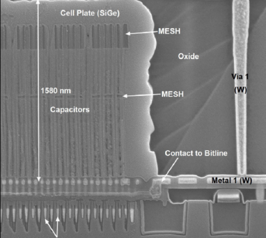
The image below shows a more recent device. Notice the much higher aspect ratio of the capacitors and the two levels of mesh required for mechanical stability. The aspect ratio of a single cell is in the range of 30:1 for the chip on the left, and it’s only getting more difficult.


3D-NAND Fabrication vs. “3D” DRAM
NAND technology has taken a hard turn away from planar design and instead now uses strings of bit cells that are formed vertically, perpendicular to the surface of the silicon wafer, rather than laying the strings out along the surface. The reason for this drastic change is that 3D-NAND is more cost effective than continuing to rely of more advanced lithography. 3D-NAND adds cost linearly based on the number of layers required in the stack, whereas continuing with lithography shrinks adds cost exponentially. The fundamental architecture of a NAND array lends itself to 3D integration where each strand of NAND bit cells is put into loops in the 3rd dimension. This is efficient because each bit line circuit is the same length.
Fortunately for NAND it was possible to go 3D and avoid the cost of Extreme Ultra Violate (EUV) lithography. In comparison, DRAM has been using stacked or 3D capacitors for over 20 years, and over this time period the capacitors have been getting taller and skinnier. It’s not possible for DRAM to go 3D because it already is. 3D-NAND is like taking a single page of paper and binding it into a 32 or 64-page book with wires connecting each letter location on all the pages through the paper. Taking DRAM and converting it to 3D would be like taking a book and stacking them 32 or 64 high, and then wiring together each letter location on just one page from each book without disturbing any of the other pages.
Can DRAM be converted into a 3D architecture like NAND? Not a chance.
How can DRAM advance?
Just like with a logic device it is possible to scale the circuitry, but the major technical challenge with DRAM includes the need to scale down the capacitors without further degrading their electrical performance. Another challenge that logic does not have to deal with is the need for DRAM to connect the circuitry below the capacitors to the metal layers and routing above the capacitors. It’s not the most difficult challenge in DRAM fabrication, but another significant difference from logic or NAND fabrication.

There is a significant economic challenge to be able to advance DRAM fabrication as well. DRAM (and NAND) are multi-sourced devices with commodity-like pricing in primary and secondary markets. This has caused DRAM to evolve into a highly available device that sells in the single digit price range ($0 to $9), whereas logic or CPU devices of similar die area sell in the multi-digit price range ($10 to $100). Really large die sell for $1000, and in some cases higher still in the case of high end FPGA devices. Considering the gross margins of the products in question, commodity memories cannot afford the high cost of advanced processing, whether EUV or advanced multi-exposure patterning, or to continue on the shrink path, because ultimately the end result is not a cost reduction. Memory is sold on a $/bit metric and if the next density DRAM costs more per bit customers will continue to use the prior generation device. This myth of Moore’s Law is that customers pay for performance, when, in reality, manufacturers produce less expensive product and have to bribe customers to adopt it with improved performance/$ metrics. Improved performance actually comes for free, just don’t tell the fanbois that.
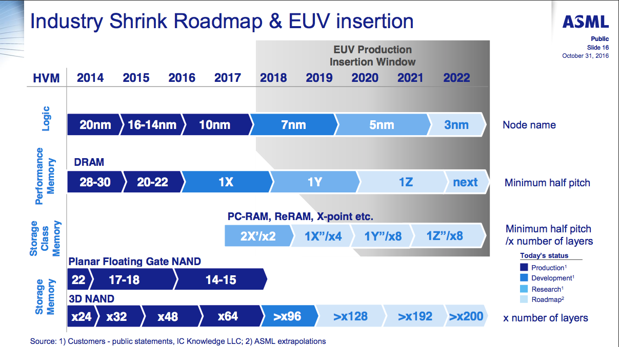
Looking at the ASML roadmap it’s quite possible that DRAM may never migrate to EUV. It’s actually amazing the DRAM has made it this far, but every good run needs to come to an end eventually, and if there had been an easy and cost effective architecture to migrate to, it would have already happened.