INSIGNIS Technology Corporation
What comes after DRAM?
DRAM is at the end of the road, having painted itself into a technology corner with nowhere to go. DRAM lithography has lagged NAND and logic because of the complexities of the capacitor construction. The roadmap from ASML, the world’s leader in lithography, shows the technology used in production for various memory types. The first 3D-NAND from Samsung appeared in production in late 2013. It’s interesting to see that NAND which has been in production since the early 1990’s converted from planar to 3D in only 3 short years. It’s likely that DRAM will follow a similar conversion, despite the roadmap showing that it will continue forever. It will be strictly an economic decision. As soon as the replacement technology drives a better financial solution for manufacturers, the legacy products will be sharply curtailed.
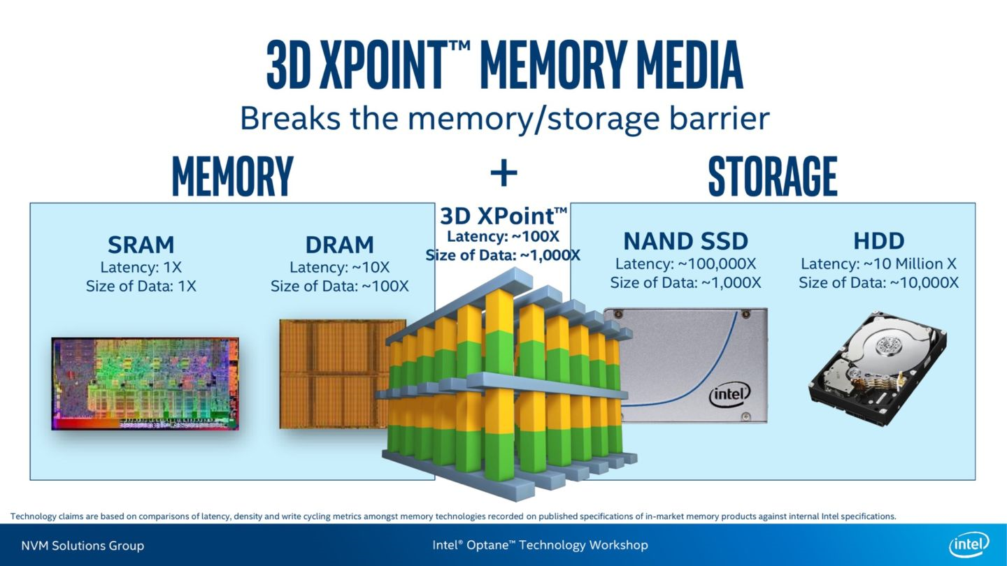
That replacement technology has been discussed for years in the general class called Storage Class Memory (SCM), as an intermediate technology between DRAM and storage. SCM is finally here, introduced by Intel in the form of 3D-Xpoint and Optane SSDs.
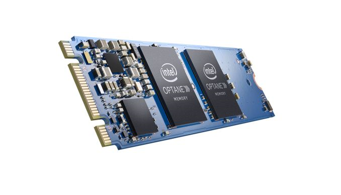
Intel’s M.2 Optane SSD was introduced in March 2017 with shipments starting in April. 3D-XP is more expensive than NAND, and putting 3D-XP behind an NVMe interface is limiting the performance of the solution. But these initial products are half the cost and volumetrically denser the DRAM. As DRAM becomes more difficult to scale, meaning it’s cost does not fall as quickly as it has historically, solutions like 3D-Xpoint will find their way into the memory hierarchy. As with any new memory technology or interface, the initial capabilities don’t represent the performance potential, but the new technology represents a solution that is scalable into the future, just as 3D-NAND has killed planar NAND.
Of course, 3D-XPoint has one more significant advantage over DRAM: like 3D-NAND, the 3D-XP circuits and bitcells can be stacked during the fabrication process. The name of the product implies it and the ASML roadmap confirms. Instead of 32, 48 or 64 layers like 3D-NAND, the 3D-XP roadmap shows a 2, 4, 8 progression. Again, stacking the layers during fabrication adds cost linearly instead of exponentially. There’s lots of road ahead for the 3D-XP roadmap and none for DRAM fabrication.
A different 3D solution: Package and Die Stacking
DRAM does still have certain performance advantages over 3D-Xpoint. It has infinite write endurance, nearly symmetric and low read-write latencies, and high bandwidth. DRAM can never be fully replaced by 3D-XPoint. Instead, expect it to migrate to dense packaging solutions either in the form of LPDDR with package on package (POP) solutions or High Bandwidth Memory (HBM) using Through Silicon Via (TSV) packaging technology as used with both Intel (Altera) in conjunction with EMIB packaging and Xilinx FPGAs with Silicon interposer technology. These direct-attach DRAM solutions, where the host processor has a direct connection to DRAM, have always been the mainstay of the off-chip memory solution and have delivered the best performance for off chip memory. Memory has focused on cost effective capacity and has been architected to maximize performance within those higher order constraints. Now, with the emergence of SCMs, the capacity of DRAM is not as critical as improving the performance. Expect future DRAM to focus on lower latency and higher bandwidth, rather than maximum capacity and lower power. Keep in mind that DRAM performance today is very poor compared to on-chip SRAM. Improving latency and bandwidth will help, but will be limited by the chip-to-chip interconnect. The solution to overcome this is to move the DRAM onto the package in the form of a multi-chip package or heterogeneous integration.
Implications for Embedded Markets and Long Term Support
Every memory manufacturer is increasing investment into NAND production and decreasing that for DRAM. Combined with the threat from 3D-Xpoint it’s entirely possible that DRAM will end as abruptly as planar NAND has, leaving the industry with DDR4 for servers, Graphics DRAM, and mobile DRAM. Embedded and legacy markets for memories will never run in the volume needed to justify a die shrink onto the most advanced process nodes. Let the buyer beware of chasing down a technology path with a finite support life from the primary suppliers, yet also one which is too expensive for secondary fabless suppliers to follow and support.
Even without the 3 big manufacturers, DDR3 is multi-sourced and manufactured in two different DRAM foundries. Without the big 3 suppliers DDR4 appears to be limited to only one foundry, one density, and quite possible two suppliers shipping the same device. It has been publicly disclosed that this foundry has ended business relationships with their process technology provider, so the likelihood of keeping pace with 8Gb capacity or DDR5 technology, if that ever materializes, it a risky proposition. DRAM process technology is highly specialized, heavily protected against infringement, and like any semiconductor process, impossible to develop quickly and independently. The chance of a new company entering the DRAM business is zero. This makes DDR4 high risk for long term assurance of supply and is not recommended for systems and markets requiring long term support.