* Klicken Sie hier um auf die nächste Seite zu kommen.
INSIGNIS Technology Corporation
Insignis' proprietary, extended test flow is engineered to produce premium quality products through our longer burn times, wider temperature ranges, and highly advanced lot, wafer, and die selection criteria.
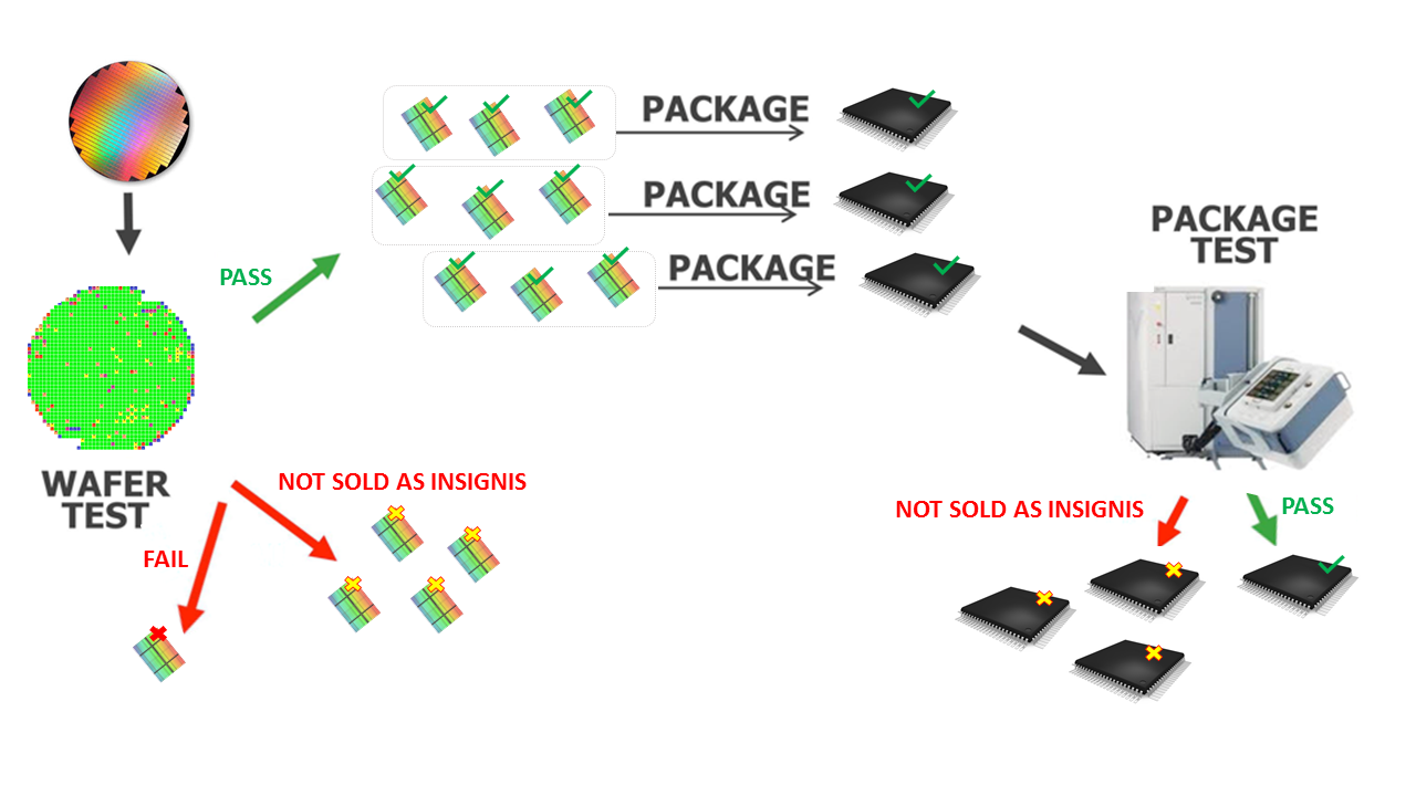
The Insignis proprietary test flow guarantees the operation of our devices at elevated junction temperatures of a minimum of 105’C through enhanced testing at multiple steps. Our burn flow is designed to stress the product at junction temperatures reaching 140°C. This removes any early life fails along with all die that have junction temperature-related fail modes.
The Insignis packaged product test flow is also engineered to guarantee the specifications are met at a 105°C junction temperature. We do this through the application of external heat on the devices such that the junction temperatures exceed 105°C during speed and margin testing.
1. We start with only the most stable fab process technology nodes.
Because of the legacy process nodes we use, we’re able to take advantage of the more stable IDS characteristics of their transistors and lower temperature sensitivities. Because these nodes have been running a very long time, they are able to be optimized based on actual device quality performance measured on large populations, unlike newer nodes which are optimized for maximizing die per wafer and emphasizing revenue over product quality. This stability of process makes them easier to produce, and with predictable quality in the end application. Our process nodes also have less current leakage, which gives Insignis products the advantage of using significantly less power than our competitors.
2. During the product development phase, our design team uses a proprietary lot, wafer and die selection process to pick only the highest quality, lowest defect material from the line.
We use the lowest defect density that meets a strict process window for the fab. When we look at a wafer or lot that comes out of the fab, we run various tests on that material to determine if it has the characteristics that meet our specification. Every part of the fab production creates devices and elements on the die. The fab then tests the structures to validate that those structures meet our specifications related to resistance, capacitance, inductance, drive, slopes of the previous parameters and thousands of others.
3. Only these premium materials continue through to testing, where we’ve developed proprietary test patterns and methodologies to assess quality.
We apply a strict, proprietary process control algorithm to our material. Our material is run through a wider range of temperatures and voltages than with standard testing, with extended burn stress and margin testing to remove material that do not meet our strict quality standards. With this proprietary test flow, we provide the lowest power, lowest operating temperature solutions to our customers, thus optimizing reliability in the field.
4. We only ship product with optimal transistor parametrics to ensure less power usage, lower temperatures, and higher reliability.
Larger, older transistors are easy to switch on and off fully. Think of a transistor as a water hose that needs to be pinched to turn off the flow of water. Newer process nodes are less able to pinch off the flow and leak a little water when the valve is off. Leakage is wasteful; in a semiconductor it consumes energy without producing any work. The energy is converted to heat which increases the temperature of the device. The increase in temperature is detrimental to device operation because it, in turn, increases the leakage of the transistors non-linearly, which again generates more heat. Some poorly designed devices have been known to go into thermal run-away which is not unlike what happens when a dam springs a leak and leads to a catastrophic failure of the entire system.
Leakage should not be confused with standby power. True, leakage is the primary source of power loss when the device is in standby, but when the device is activated the leakage is not “exchanged” for active power. Even when a memory chip is running at maximum performance, less than 1% of the billions of transistors are activated and the other 99% continue to leak. The total power of the device is the active power which is added on top of the leakage power. Minimizing leakage power is the single most important transistor design problem of the last decade. Since the newer transistors are physically smaller, it is more difficult to get them to turn off completely. In a logic process used to build CPUs or ASICs, the process technology has migrated to FinFET, Tri-gate, or FD-SOI transistors to overcome this leakage problem. These new transistor technologies were introduced at 22nm and are in place in all logic fabrication nodes at 16nm. Unfortunately, given the manner in which DRAM are constructed, it’s just not cost effective to adapt these more complex transistors in a DRAM fabrication process.
In summary, one of the unintended consequences of newer, faster, advanced process nodes is the significant increase in leakage current. With all semiconductors, high temperatures and fail rates are directly linked to leakage, but heat is particularly bad for DRAM. Higher temperatures lead not only to decreased semiconductor reliability, but also lead to soft error rates related to reduced data retention time and increased probability or Variable Retention Time (VRT) errors. The reduction of leakage is a significant benefit of being on the established, mature technology as compared to the leading edge. Insignis has implemented strict, proprietary design and test processes to keep the DRAM temperature as low as possible, ensuring the best quality product for our customers.
For more details about our Extended Test Flow process, click here.