* Klicken Sie hier um auf die nächste Seite zu kommen.
INSIGNIS Technology Corporation
Abstract
As semiconductor manufacturing runs headlong into economic and technical challenges, the markets that can afford to amortize the costs and assume the risks of bleeding edge technologies become smaller. At some point the entire industry will bifurcate into a legacy and specialty market - one that is able to cross the chasm into new memory devices and architectures. DDR4 may look like a commodity now, but once the remaining 3 DRAM technology developers move on to the next big thing, there is no licensee or foundry able to support advanced DDR4 in a competitive marketplace. Consider legacy DRAM supported by secondary and fab-less DRAM makers today with devices selling at a price 2x to 5x their historic lows, and then consider a specialty device like RLDRAM selling for a 5x higher premium. DRAM makers have been waiting for sufficient market consolidation to be able to finally raise their profit margins to CPU manufacturer levels. That time will be here sooner than you can imagine.
Introduction
Industrial applications are designed to perform a specific function in a reliable manner and in harsh environments, and the performance requirement is fixed for the life of a product. It is true that a newer, replacement system for a RT application may be higher performance, but for one that is in service in the field, that is not the case. Most embedded applications do not benefit from the rapid advancement of system performance by moving to the newest processors and memory technology. They continue to ship legacy CPUs and controllers from well-established suppliers and require long term support for the peripheral components such as memories.
Moving these applications to advanced semiconductor fabrication processes and faster device designs can prove to be problematic. The newer devices can be more susceptible to minor perturbations from system circuit noise and similar disturbances from high energy particles or cosmic radiation due to increased voltage regulation, lower core voltage, and faster edge rates. Some of the observed failure mechanisms can be designed-out or worked-around in new memory controllers or implementations, but systems already in the field don’t have that option. Memories used in applications designed years ago with now mature controllers need memory that meets the reliability and quality expectations of the original design.
The major, high volume memory suppliers will continue to support legacy functionality by migrating devices to a more advanced process node, but will only do so if it continues to make economic sense. They will promise to support indefinitely until the day it is determined to be the end of the line for a product, and then the dreaded last time buy appears without warning. Most astute customers recognize the peril this places them in and will migrate to alternative long term suppliers well in advance so the customer can establish run rates and favorable terms for extended support. In addition to the obvious business advantages, there are technical reasons to avoid die shrinks.
DRAM design and fabrication
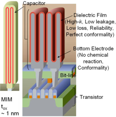
A DRAM stores data on a capacitor that is isolated by a ‘pass’ transistor. This combination is referred to as the bit cell with each one having x and y dimensions of a few tens of nanometers. The capacitor is fabricated in the space above the circuitry, and in modern DRAM bit cells, the capacitor resembles a tall, thin-wall cylinder, with the dielectric on both the inside and outside surfaces of the tube. As the process geometry shrinks, it becomes easier than ever to upset the value on a bit cell either by disturbing the capacitor, the pass transistor, or the bit-line which connects to the sense circuitry. The sense operation measures millivolts of differences caused by a small capacitor driving a large bitline. The bitline is connected to hundreds of pass transistors and the parasitic capacitance of the bitline itself can be more than 10x larger that the bit cell capacitor.
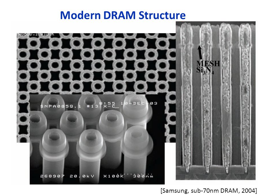
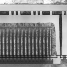
The diagram to the right doesn’t do justice to the complexity of the DRAM capacitor array. The capacitors are so tall they need to be mechanically stabilized with a mesh so the spacing between them doesn’t vary, otherwise the charge of one capacitor can corrupt an adjacent one. Below is an image from 2004 where the capacitors are short and stubby compared to current device technology, and includes a silicon nitride mesh which stabilizes the location of the capacitor during device fabrication. Without the mesh, the capacitors would lean over and contact adjacent cells.
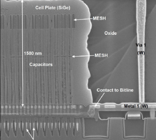
The image below shows a more recent device. Notice the much higher aspect ratio of the capacitors and the two levels of mesh required for mechanical stability. The aspect ratio of a single cell is in the range of 30:1 for the chip on the left, and it’s only getting more difficult.
3D-NAND Fabrication vs. “3D” DRAM
NAND technology has taken a hard turn away from planar design and instead now uses strings of bit cells that are formed vertically, perpendicular to the surface of the silicon wafer, rather than laying the strings out along the surface. The reason for this drastic change is that 3D-NAND is more cost effective than continuing to rely of more advanced lithography. 3D-NAND adds cost linearly based on the number of layers required in the stack, whereas continuing with lithography shrinks adds cost exponentially. The fundamental architecture of a NAND array lends itself to 3D integration where each strand of NAND bit cells is put into loops in the 3rd dimension. This is efficient because each bit line circuit is the same length.
Fortunately for NAND it was possible to go 3D and avoid the cost of Extreme Ultra Violate (EUV) lithography. In comparison, DRAM has been using stacked or 3D capacitors for over 20 years, and over this time period the capacitors have been getting taller and skinnier. It’s not possible for DRAM to go 3D because it already is. 3D-NAND is like taking a single page of paper and binding it into a 32 or 64-page book with wires connecting each letter location on all the pages through the paper. Taking DRAM and converting it to 3D would be like taking a book and stacking them 32 or 64 high, and then wiring together each letter location on just one page from each book without disturbing any of the other pages.
Can DRAM be converted into a 3D architecture like NAND? Not a chance.
How can DRAM advance?
Just like with a logic device it is possible to scale the circuitry, but the major technical challenge with DRAM includes the need to scale down the capacitors without further degrading their electrical performance. Another challenge that logic does not have to deal with is the need for DRAM to connect the circuitry below the capacitors to the metal layers and routing above the capacitors. It’s not the most difficult challenge in DRAM fabrication, but another significant difference from logic or NAND fabrication.
There is a significant economic challenge to be able to advance DRAM fabrication as well. DRAM (and NAND) are multi-sourced devices with commodity-like pricing in primary and secondary markets. This has caused DRAM to evolve into a highly available device that sells in the single digit price range ($0 to $9), whereas logic or CPU devices of similar die area sell in the multi-digit price range ($10 to $100). Really large die sell for $1000, and in some cases higher still in the case of high end FPGA devices. Considering the gross margins of the products in question, commodity memories cannot afford the high cost of advanced processing, whether EUV or advanced multi-exposure patterning, or to continue on the shrink path, because ultimately the end result is not a cost reduction. Memory is sold on a $/bit metric and if the next density DRAM costs more per bit customers will continue to use the prior generation device. This myth of Moore’s Law is that customers pay for performance, when, in reality, manufacturers produce less expensive product and have to bribe customers to adopt it with improved performance/$ metrics. Improved performance actually comes for free, just don’t tell the fanbois that.
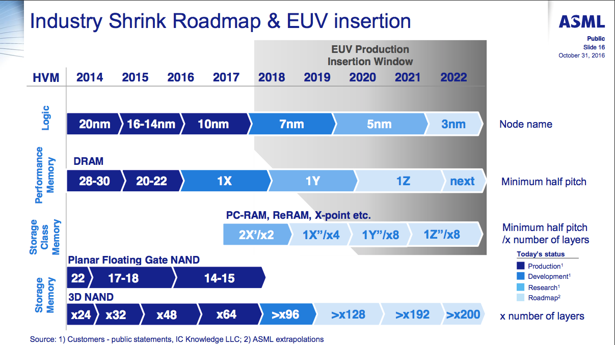
Looking at the ASML roadmap it’s quite possible that DRAM may never migrate to EUV. It’s actually amazing the DRAM has made it this far, but every good run needs to come to an end eventually, and if there had been an easy and cost effective architecture to migrate to, it would have already happened.
What comes after DRAM?
DRAM is at the end of the road, having painted itself into a technology corner with nowhere to go. DRAM lithography has lagged NAND and logic because of the complexities of the capacitor construction. The roadmap from ASML, the world’s leader in lithography, shows the technology used in production for various memory types. The first 3D-NAND from Samsung appeared in production in late 2013. It’s interesting to see that NAND which has been in production since the early 1990’s converted from planar to 3D in only 3 short years. It’s likely that DRAM will follow a similar conversion, despite the roadmap showing that it will continue forever. It will be strictly an economic decision. As soon as the replacement technology drives a better financial solution for manufacturers, the legacy products will be sharply curtailed.
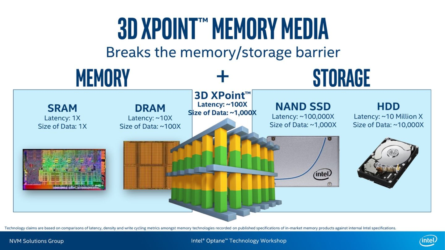
That replacement technology has been discussed for years in the general class called Storage Class Memory (SCM), as an intermediate technology between DRAM and storage. SCM is finally here, introduced by Intel in the form of 3D-Xpoint and Optane SSDs.
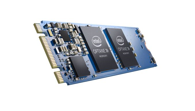
Intel’s M.2 Optane SSD was introduced in March 2017 with shipments starting in April. 3D-XP is more expensive than NAND, and putting 3D-XP behind an NVMe interface is limiting the performance of the solution. But these initial products are half the cost and volumetrically denser the DRAM. As DRAM becomes more difficult to scale, meaning it’s cost does not fall as quickly as it has historically, solutions like 3D-Xpoint will find their way into the memory hierarchy. As with any new memory technology or interface, the initial capabilities don’t represent the performance potential, but the new technology represents a solution that is scalable into the future, just as 3D-NAND has killed planar NAND.
Of course, 3D-XPoint has one more significant advantage over DRAM: like 3D-NAND, the 3D-XP circuits and bitcells can be stacked during the fabrication process. The name of the product implies it and the ASML roadmap confirms. Instead of 32, 48 or 64 layers like 3D-NAND, the 3D-XP roadmap shows a 2, 4, 8 progression. Again, stacking the layers during fabrication adds cost linearly instead of exponentially. There’s lots of road ahead for the 3D-XP roadmap and none for DRAM fabrication.
A different 3D solution: Package and Die Stacking
DRAM does still have certain performance advantages over 3D-Xpoint. It has infinite write endurance, nearly symmetric and low read-write latencies, and high bandwidth. DRAM can never be fully replaced by 3D-XPoint. Instead, expect it to migrate to dense packaging solutions either in the form of LPDDR with package on package (POP) solutions or High Bandwidth Memory (HBM) using Through Silicon Via (TSV) packaging technology as used with both Intel (Altera) in conjunction with EMIB packaging and Xilinx FPGAs with Silicon interposer technology. These direct-attach DRAM solutions, where the host processor has a direct connection to DRAM, have always been the mainstay of the off-chip memory solution and have delivered the best performance for off chip memory. Memory has focused on cost effective capacity and has been architected to maximize performance within those higher order constraints. Now, with the emergence of SCMs, the capacity of DRAM is not as critical as improving the performance. Expect future DRAM to focus on lower latency and higher bandwidth, rather than maximum capacity and lower power. Keep in mind that DRAM performance today is very poor compared to on-chip SRAM. Improving latency and bandwidth will help, but will be limited by the chip-to-chip interconnect. The solution to overcome this is to move the DRAM onto the package in the form of a multi-chip package or heterogeneous integration.
Implications for Embedded Markets and Long Term Support
Every memory manufacturer is increasing investment into NAND production and decreasing that for DRAM. Combined with the threat from 3D-Xpoint it’s entirely possible that DRAM will end as abruptly as planar NAND has, leaving the industry with DDR4 for servers, Graphics DRAM, and mobile DRAM. Embedded and legacy markets for memories will never run in the volume needed to justify a die shrink onto the most advanced process nodes. Let the buyer beware of chasing down a technology path with a finite support life from the primary suppliers, yet also one which is too expensive for secondary fabless suppliers to follow and support.
Even without the 3 big manufacturers, DDR3 is multi-sourced and manufactured in two different DRAM foundries. Without the big 3 suppliers DDR4 appears to be limited to only one foundry, one density, and quite possible two suppliers shipping the same device. It has been publicly disclosed that this foundry has ended business relationships with their process technology provider, so the likelihood of keeping pace with 8Gb capacity or DDR5 technology, if that ever materializes, it a risky proposition. DRAM process technology is highly specialized, heavily protected against infringement, and like any semiconductor process, impossible to develop quickly and independently. The chance of a new company entering the DRAM business is zero. This makes DDR4 high risk for long term assurance of supply and is not recommended for systems and markets requiring long term support.